I also think that Vivado compatibility is important factor, if not a critical one.
Interesting posts;
I am also looking for some solution to the problems of fast data transfers between FPGA and some data processing unit. I am using fast ADC data acquisition, with some numerical pos-processing. Just recently I have tried the soft riscv on the Digilent Arty100 board (while waiting for the Pt board to come), and found it disappointing.
About 15 years ago I have used STM32F chip with a bit of FPGA memory mapped just above the STM static RAM to move data between these two. It still works nicely.
This time I plan to use STM32H7S7L8 (660MHz Cortex M7) paired with the APS256XXN “hexa-spi” RAM, accessing some 32k FIFO in the Artix100 chip in a burst mode (no address switching required, just data). Assuming 200 MHz access rate, fast connectors, and robust data cache on the STM chip, that may work …rather fast.
As usual, I will curse myself for undertaking this project, but it may work. Will be happy to report the mishaps and failures, but wouldn’t it be nice to have a Pt-compatible little processor board?.
The Raspberry Pi 5 has a PCIe 2.0 lane exposed. The Pt should be able to use this to get 500MB/s between the two. I’m looking into make a board for this. It’s a shame it’s only one lane as the Pt could do up to 4.
I was about to suggest this too XD
The Pi 5’s SOC seems to have 5 PCIe 5 lines but 4 of them are used internally to connect the RP1 southbridge.
Kinda sad that more lines could have been exposed and made available when some peripherals are not used such as the MIPI, but i don’t know how much work it would have needed to achieve this.
I am not sure about the thermal characteristics, so take this reply with a grain of salt, but I have a Pynq Z2 FPGA Board, and it looks like they just slapped a small heatsink on the chip and called it a day. The chip does get noticeably warm, but reaches a point at which it does not get warmer, and works fine. I have seen some people use it without a heatsink, and the Pynq Z1 does not usually have a heatsink. I do not know how bad the thermal is on the Pt, but maybe you can just get away with a heatsink on it.
The Pynq Z2 uses a speedgrade 1 Zynq with 85k cells and does not seems to have GTP.
The Pt will have a speedgrade 2 and 100k cells and GTP, so basically more elements and elements that runs faster.
Of course, the power level is directly dependent on your design : the more cells used and the higher the frequencies, the higher the power usage, therefore the higher heat.
So the need of an heatsink is bound to your design ![]()
The way I see it, the Pt needs a fan. I was thinking maybe it can be clipped onto the side, or on top of the heatsink and have an attachment that has a hole in it for the fan to go in, and then you can stack boards on top. Like I said, I am just getting started in the world of electronics, so my opinions and ideas do not mean much yet.
I just put in my preorder! Black Friday, it’s traditional! I ordered Au, Ft, Hd, and a v1 converter board. I’m mostly curious to see if the higher speed grade results in an improvement to the SDRAM latency. On the lower speed grade, the MIG interface is only getting clocked at 81.25MHz, I assume because some pipeline stage that can’t be broken down further can’t complete within a 100MHz cycle. But on higher grades I think you can generate a core which can support 100MHz. I’m sure the actual improvement will be modest, the bulk of the latency is just waiting on the sdram after all. But it should help!
Yeah the new speed grade supports 800 MT/s instead of 667MT/s so a nice little bump there.
is pinout of Alchitry Pt available, please?
This is a very rough draft for the schematic. The actual pins used will be swapped around during layout but the basic function of each pin should stay the same (ie clock pins, dual voltage, LVDS, ADC, pins stay where they are).
PtSchematicDraft.pdf (205.1 KB)
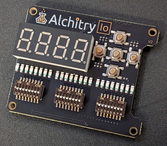
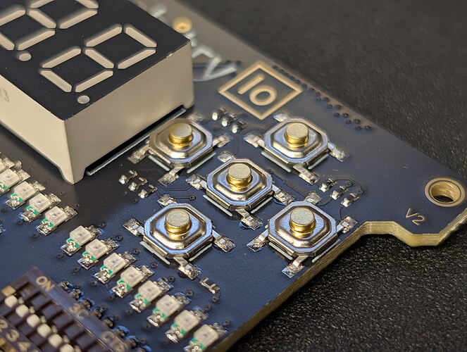
The Io prototypes have arrived! They look pretty great and I’m excited to actually get to test them out once the Au prototypes arrive in the next couple of days.
I used a different button that has a taller plunger and a more noticable click. It’s a nice improvement.
Thanks for pinout. I see some changes (against to Au) at FT2232HQ second usb channel. What is your plan to use/configure it, please?
By default I think it’ll be setup just as a serial port like the Au. You’ll be able to flash the EEPROM to switch it to the FIFO interface. (Should be doable via a single click in Alchitry Labs)
The FIFO being an optional setup instead of the default makes sense as it’ll require a custom program using D2xx instead of just a generic serial port.
Also, if I can quickly mention, on the old Au, there is one inductor that is taller than the connectors. My extra Aus inductor is cracked, and the first Au I got I returned because the inductor was cracked. If you could use a smaller inductor that would be great, but you probably can not because you already designed the boards.
I have a question about JTAG : Is it possible to add a device to the JTAG chain by doing some routing in the FPGA?
If not, is it conceivable to add a jumper that could be used to open the chain?
About new elements, is there plans for a level-shifting one?
It could take an external voltage on the high side and 3.3v from the board on the low side?
I couldn’t find a level-shifter chip that allow “free” voltage on both side, there always an high side and a low side, do you know if a chip that can accept any voltage on both side exists?
For exemple 5v to 3.3v but also 2.5v to 3.3v?
I’m still working on interfacing to an ATA device (5v signals) and it’s pretty messy on the breadboard XD
I will build an adapter that will plug on the Br for now, it will save a lot of jumper wire mess XD
If you are looking for power conversion, you can use a chip that I am currently using to make a board for a project: the LMR38020FDDAR
For signals, I am pretty sure that you can just slap a bunch of transistors on a board and call it a day.
I’m searching for signals with kinda high speed (as I said, ATA signals for now).
I’m using TXS0108E for my testings, it works for me because I can do 3,3v on side A to 5v on side B, and only this way : there is a restriction that side A must be <= side B.
My question was about the existance of a chip that allows any combination, which would allow to a fixed side at 3.3v for the FPGA, and allows to us to have something higher or lower on the other side.
It looks like the TXB0304 allows this symmetrical usage, but it’s 4 bits and limited to 3.3v.
Thanks for the power converter, I’ll keep the number around, I may need one later ![]()
I am sort of confused, because I am pretty sure you can find high speed transistors and maybe add filtering capacitors, and don’t transistors work at low to higher voltages (or any voltage you want, externally powered)? Also instead of having ICs with extra components, it should be cleaner.

