For those of us that never noticed the pins on bank 34 don’t work until long after the 30 day warranty??? how to repair board ?? help us out @Alchitry. instructions on soldering/repairing the boards? sparkfun said go screw.
Could be pretty hard and will most likely requires a heat gun, some kapton tape to protect surrounding components, probably some flux and possibly tweezers, and to be very carefull.
According to @alchitry on the other topic, the issue comes from the voltage switch being improperly soldered.
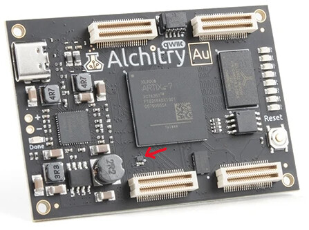
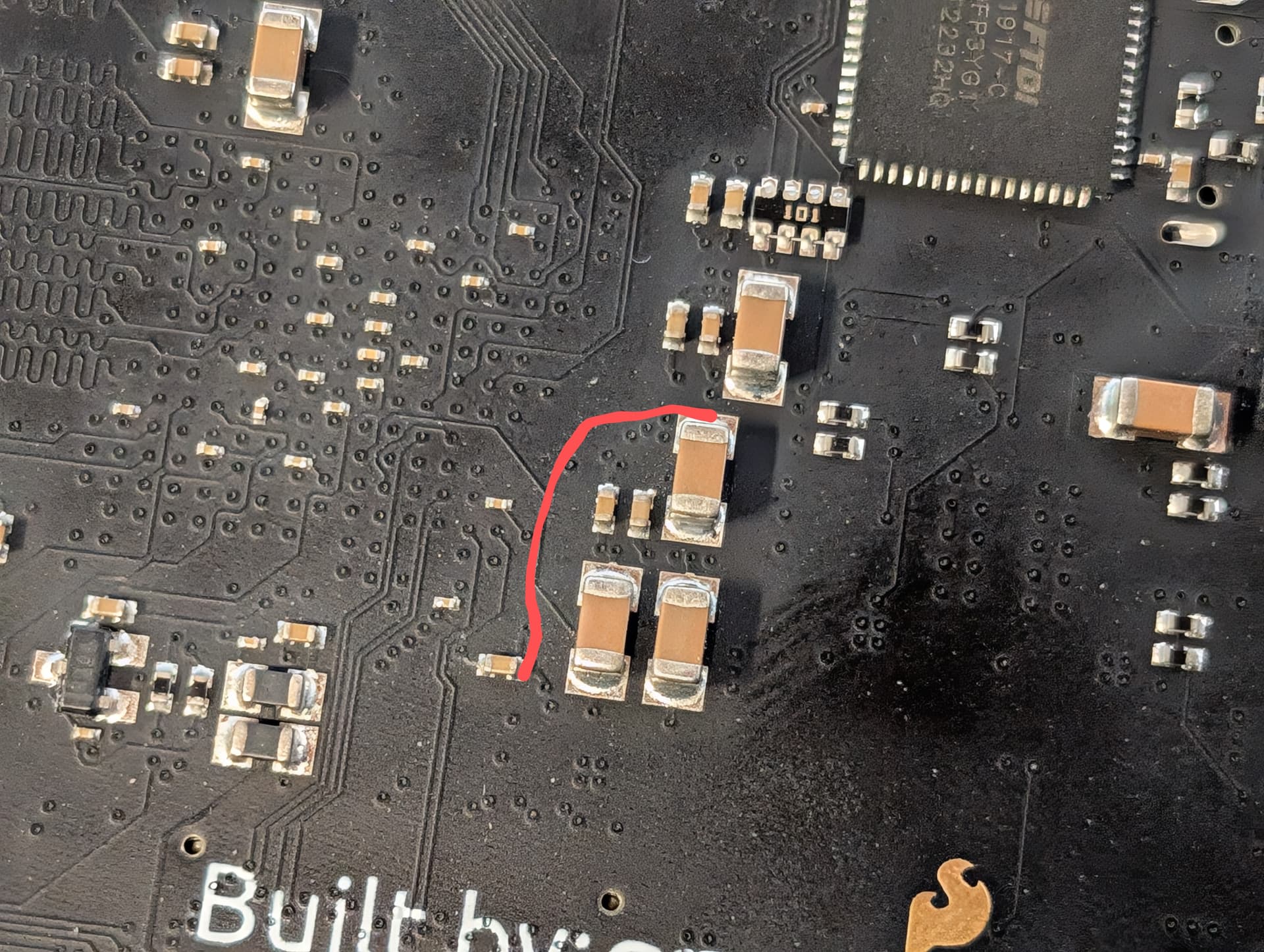
Can you see this tiny black square near the C-bank connector?
This is the said voltage switch, it’s a 6-pin BGA, and it’s this part that need to be reworked.
You probably understand how hard it will be to fix this, and why @alchitry suggested to ask SparkFun for a replcement instead.
The major issue here is that soldering BGA by hand will be hard, and there are risks that the heat cause damages to the PCB, the C-bank connector nearby or weakens the solder balls of the FPGA nearby…
If you don’t use VBSEL, maybe it would be possible to bypass the switch with a wire, but @alchitry will know better.
The easiest way to “fix” this is to just bypass the switch (if that’s acceptable).
If you’re seeing 0V, it’s probably safe to jump the output to 3.3V and have everything work. The safest method would be to remove that tiny black chip @gc74 pointed out with a hot air gun then jump the power.
You then have two options, if you removed the switcher, you can jump two of the pads. The top right, VB34, and the bottom right, +3V3.
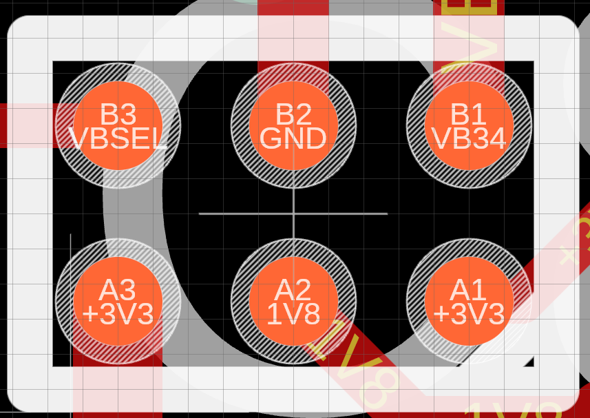
Otherwise, you can solder a wire between these two points.
However, given this is clearly a defect and I think your board should be replaced, you can contact me at justin@alchitry.com and I’ll arrange a replacement with an Au V2 if that’s acceptable.