I don’t understand what’s going on here.
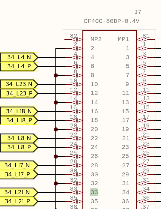
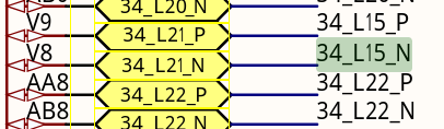
What’s the difference between the yellow and the black label and why do some of them not match?
What’s the difference between the yellow and the black label and why do some of them not match?
Also why does the numbering along the left side of J7 switch from even numbers to odd numbers between pins 32 and 33?
What does this mean physically?
How does this mate with the Br board?
You can ignore the black text. They should match but it was just used as a work-around for an issue in Altium.
Excellent catch with the pin number mistake. This was left over from when pins were swapped around during layout. I thought I had re-ordered them all correctly but that pair is clearly wrong.
Go off the actual pin number and not the location. That group should be swapped with the pair on the other side of the connector.
I’ll update the schematic and get it uploaded today.
As for how it mates with the Br, the bottom side and top side connectors are mirrored. That means pin 2 mates with pin 1. The locations on the header in the schematic should match (pin 2 is top left for bottom side, pin 1 is top left for top side, those connect).
UPDATE: The corrected schematic is now live.