I have a design where I’m driving out of the Pt on pins W7 and V7.
These should correspond to bottom side bank B pins B27 and B29.
That’s IO_L19N and IO_L19P in the IO Planner.
That’s 34_L19_N and 34_L19_P on the schematic.
But when I probe the board I see the signals on B28 and B30.
Is there a schematic and/or layout mismatch somewhere that is already known?
If not, could somebody try to reproduce this independently by routing a signal to pin W7 and tell me where they see it on the breakout connector?
Are there gerber images available for review? That would be easier than buzzing these on the bench.
I’m going to go buzz out the boards from pin to pin and I’ll report back. But it seems I can’t trust the silk screen vs the schematic. I hope I just did something dumb, but I can’t see how this isn’t a layout or silk screen issue.
I won’t tell you how many hours I spent looking for my mistake in my hdl, in simulation and in the schematic, and in the forums, and in the web pages for the boards and in the vivado design checkpoint. I’m glad the solution is so simple!
Thank you for saving me the final step of buzzing out the pins.
Thinking of the metaphysics here…
How is this discoverable? Is it not the job of the schematic to allow this type of signal traching? Is this not a giant failure on the silk screen to not match the schematic?
How could I have learned about the mapping file? How is that discoverable?
Could I boldly suggest renumbering the schematic to match the silk screen? Or adding a text note in the schematic saying “silk screen numbering is off by one”?
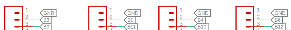
I just looked at the schematic again. Just for future reference: this is not an off by one problem. The first four pins are B3, B5, B4, B6. But the silk screen for the B connector seem to be 3,2,4,6, or maybe it’s 6,4,2,3? I can’t tell you just looking at the mapping file the schematic and the silk screen! There is literally no way to know how this is mapped without the mapping file. Not only that, the pin mapping file maps to the FPGA pin numbers, not the connector pin numbers, so you also need to look at the Pt schematic to cross-reference if you want to know what connector pin it actually goes to.
Wild. There must be some ‘history’ that led to this scrambled mapping.
But the mapping file isn’t one of the documents listed on the board page. It’s far too easy to assume, like I did, that a connector with numbers would match the pin numbers if there is no obvious warnings and links to a pin mapping file.
In a situation like this, I’d think the schematic should be annotated with the text of every single silk screen reference. Is this in kicad? Is the source code open so I could add the annotations and contribute back?
I just found out by realizing that on the top side, the BR numbers matches the schematic numbers, and on the bottom side, the pin numbering on the bottom side are mirrored.
That means this is probably because the connector is on the bottom, making it actually upside down, which explains why the connector’s numbering is mirrored.
About the apparent scrambling of the pins on the BR, this is made on purpose because the pins are routed to support differential pairing.
For exemple : B3 and B5 forms a pair, surrounded by grounds. Same goes for B4 and B6.
Huh? Am I confused? The BR numbers on the top do not match the schematic numbers in my picture. For example where is B5?
I agree: it’s good that the diff pairs are routed next to each other. But that only explains the “scrambling.” Not the conflicting numbering between silk screen and schematic.
I also have beef with the “surrounded by grounds” routing. It doesn’t seem to be done well. But that’s for another post.
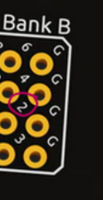
Aha! I just noticed the rendering on the Br product page has typos in it such that it doesn’t match my actual board. e.g. in the screen shot here it shows 2, but on my board it shows 5.
Thanks @gc74. It all makes sense now. I re-soldered all my connections to swap them.
I do think the Br schematic should have a note near the bottom side connectors to clarify this, as it was too easy for me to look at the pin numbers and get the wrong pin on the board because I expected the number of the bottom side connector should match the silk screen.
It might say something like:
“The numbers on the bottom side silk screen are swapped relative to the connector pinouts on J1, J5 and J6. (e.g. pin J5.3 is labelled 4, pin J5.4 is labelled 3, J5.6 is labelled 5, J5.5 is labelled 6, etc.)”
I need to update the Br render. That’s from an old rev that had the naming mistake.
The bottom connectors are a little confusing in the schematic since the pin names are based on the top connectors that they would mate to. That makes the bottom connector’s numbers mirrored. Pin 4 is A3 and pin 3 is A4. I’ve updated some of our library components to use the Alchitry pin numbers but I haven’t updated the board’s schematics.
There shouldn’t be a B2 on the Br. @gc74 do you have a board that has a 2? Or did you just mean pin 2 on the Br’s header? (an early batch was misnumbered but I don’t think those shipped).
No worries. These things are minor in the grand scheme of things. So far I’m very happy with the way this is going. Great work!
Since I started with a design that needed the GTP pins I never did anything with the top side of the board, top side connectors or top side pinouts, so it didn’t occur to me that they wouldn’t match the pin numbers. It’s “obvious” once you look at the top that you can’t have it both ways. Ha.
That said, a note on the Br schematic about the silk screen would have avoided this and would be a boon for future users.
There is no 2 on the B connector. I used the rendering as a reference for the bottom side because there is no bottom side photo posted on the product page and it was easier than grabbing a camera. I was confused until I saw that the rendering didn’t match the board.
I generally plan my wiring by drawing over a photo or rendering. All is going fine now after swapping all my wires. The gtp is passing data. I’m working on streaming through via the USB FIFO. It is dropping data but the full flag is never going high, so I need to spend some time debugging.