I adopted the Mojo V3 back in 2016 as a base for a factory test jig which is still in use today. Now that Xilinx sorted out the situation with Samsung Foundry for fab space, Spartan-6 FPGAs are available once again after a big shortage. I thought it couldn’t hurt to make a few extra boards as a backup, so I took a look at the Mojo V3 Eagle files available here.
The PCB layer stackup shown in these files is very strange:
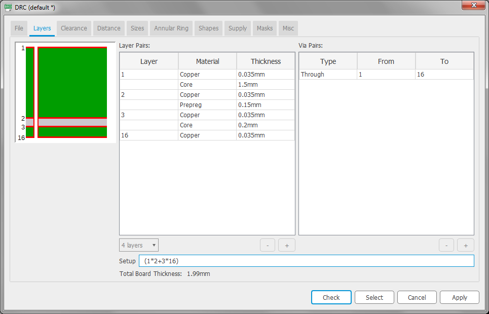
First, I’ve never seen a stackup that’s this asymmetrical. A clue that makes me think something is wrong is that the overall thickness adds up to 1.99mm, but my caliper measurement on a physical Mojo V3 board reports 1.56mm. Do you know what’s going on here and what is the correct stackup for this PCB?