Maybe we could hook a logic analyzer on the SPI bus and see what the Vivado’s bridge do, sadly I don’t have a fast enough one and I’m afraid of damaging my Au ![]()
How fast of a logic analyzer is need?
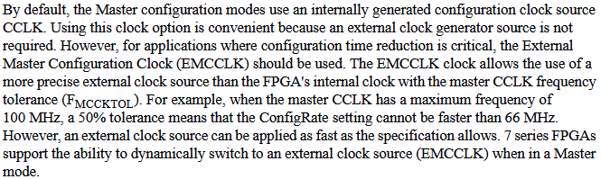
It looks like the FPGA’s CCLK starts at 3 MHz read the bitstream header, and then switch to the value provided by the ConfigRate field defined when the bitstream was generated, which defaults to 3 MHz but can go up to 66 MHz.
So we don’t need a big beast, and after better looking, I have one of these cheap 24 MHz usb ones (I thougt it was much slower) that may be enough, but I still have to hook it on the flash ship without damaging my Au, since the SPI bus is dedicated for this and thus not exposed on the connectors.
I may try it when I find some time ![]()
I found out on AMD’s forum that CCLK is said to have a pretty wide tolerence (up to 50%??? ![]() ).
).
So when the configuration time is important, they highly recommend to use an external master clock, which is done by feeding a clock on the EMCCLK pin.
The FPGA will default to it’s internal oscillator, and an field in the bitstream tells it to switch to the external clock.
The flash chip we use is rated for 104 MHz, so maybe we could get better configuration time by connecting the 100 MHz to the EMCCLK pin?
Here is the relevant section in Xilinx’s doc :
From UG470, page 32
EMCCLK is not a dedicated clock capable input so the 100MHz clock would need to be routed to it and to it’s normal pin. This would sacrifice an IO pin. Doesn’t seem worth it for a very marginal gain that the vast majority of people don’t care about.
I’ll probably have some time this week to hook up my logic analyzer to the board and grab some waveforms.
Oh, I didn’t saw the EMCCLK can be used as an IO, the doc is so big (which is expected for such complex and feature-rich devices), that I maybe read like… 5% maybe? ![]()
I’m sorry if I make stupid or wrong suggestions ![]()
No worries! I’m still learning new things about them all the time too.
Much appreciated.
I must have one of the early Au v2 boards. Here’s what I had to do, working with vivado 2025.1 on 64-bit linux:
VIV=/path/to/vivado
# use packaged rlwrap instead of the broken rlwrap bundled with vivado
BNDL=$VIV/bin/unwrapped/lnx64.o
mv $BNDL/rlwrap $BNDL/rlwrap.old
sudo apt-get install rlwrap
ln -s `which rlwrap` $BNDL/rlwrap
# after plugging a USB cable from host to the Alchitry board
# disconnect the default SIO driver from /dev/ttyUSB{1,2}
sudo modprobe -r ftdi_sio
# program the FTDI chip on the Alchitry board
# NOTE: quoting of multi-token-strings doesn’t work properly
# I suspect the script, but haven’t looked. I just used dashes instead of spaces
$VIV/bin/program_ftdi -write -f FT2232H -v Alchitry -b Alchitry-Au-V2 -d Alchitry-Au-V2 -s 000000
# it seems I still needed to run this by hand, for Vivado HW mgr to talk to:
# running it privileged so it can access /dev/ttyUSB* so devices are detected
sudo $VIV/hw_server &