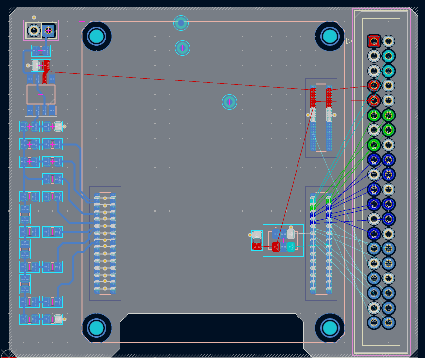
Hello,
I’ve got a custom Element board I’m putting together for the Alchitry Cu V2. It’s intended to handle composite video generation for a CRT TV and interface with an 8-bit computer. On the left side I have an R2R DAC and op-amp, which were easy enough to route. It’s the right side that’s giving me some trouble.
I’m intending to interface this board with the main 8-bit computer motherboard through a standard 40-pin IDC ribbon cable, so I have a 2x20 IDC box header on the right side with various signals that need to be passed between the two boards (data lines, address lines, power, ground, etc). These signals will be coming primarily from Bank A (with 5V, 3.3V, and the “FPGA done” signal coming from the control header).
Does anyone have any tips on how to handle routing between the fine pitch connector and the large through hole connector? I’ve been at it for a few days but am struggling to get a result that doesn’t have a bunch of clearance violations. The positions of the signals on the Bank A connector are flexible, so I can reprogram them for whatever pins make this the easiest. The pinout of the 2x20 header is also fairly flexible; the motherboard hasn’t been finalized so I can still shuffle signals around, though I’d like to keep the ground signals as interleaved as possible.