Hi All
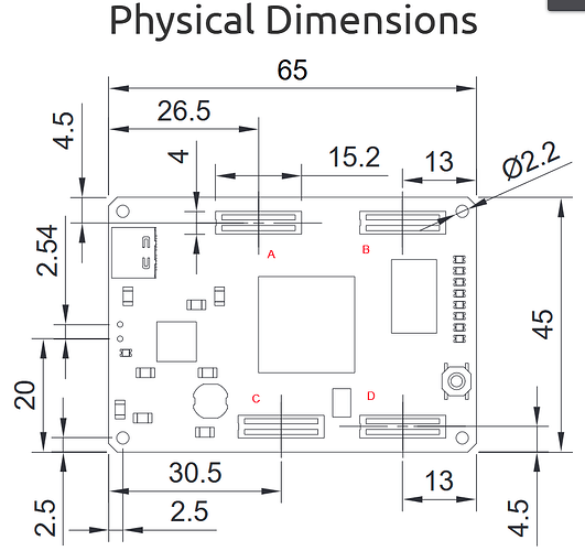
I have just started and wish to interface the Au version 1 to my own hardware. however the mechanical drawing supplied shows the position of the connectors but not which connector is bank A B C or D on the schematic. Can any one help? my next question is where can I find a constraints file for Vivado that lists the schematic connector banks a b c d pins for all the Atrix chip IO.
T[date=2025-03-13 timezone=“Europe/London”]hanks
Did you look at the page for Sparkfun?
https://cdn.sparkfun.com/assets/3/7/6/b/9/AuDrawing.pdf
I don’t see anything referencing Banks C or D, only A, B, and Control so maybe I’m looking in the wrong spot, but it seems to have the pinouts and full drawings where the things are connected.
These are for V2, which have the new connectors.
That’s why there is no C and D.
Here is the schematic for V1 :
https://cdn.sparkfun.com/assets/a/2/2/0/a/alchitry_au_sch_update-2.pdf
And here is the pinout sheet for V1 :
The connectors are in this order on the board :
Thank you, I assume that pin one is left bottom of each connector on the provided drawing as per the IC convention the little bobble on the end represents the pin one end?
much appreciated.
Thanks, This is version 2 info and I have a version 1 this accounts for the discrepancy
If you’re using KiCAD, there is a symbol and footprint with the connectors lined up perfectly (see my other post).
As for a constraints file I have this, I seem to recall that BA48 and BA49 may be reversed.
p.s. hi from a fellow brit (assumed from the time code).
AlchitryAuWithBR.zip (1.8 KB)
KiCAD library (which I’ve used) is here - GitHub - Lopfi/alchitry-element-kicad: A KiCad library for shields for alchitry fpga boards
Yep a fellow brit - Thanks for the file I will use as a template and check the connections to my kicad schematic. It will give me confidence that the assumptions I have made for the schematic are correct.
Mike
