If I output the SPI data out bit one clock cycle after the reading edge (in Mode 1) instead of waiting for the writing edge in spi_peripheral.luc, the speed increases from 17 MHz to 21 MHz. Makes sense I think.
With this change this goes up to 23 MHz in Mode 2, while Mode 1 and Mode 3 totally fail (also makes sense).
I had been meaning to ask what kind of connection quality you were working with. At the frequencies you’re trying to go at, I would blame jumper wire connections before I would blame the chips.
The connections to the Ili9341 display were identical and gave no problems at 30 MHz. But I think the timing constraints with bit banging and sampling sck instead of hardware spi made the jumper wire connection quality more critical.
The main problem was a flaky ground wire connection that caused problems above 16 MHz with the Teensy.
With a 300 MHz (clock wizard) SPI sample clock it works reliably up to 39 MHz.
So the jumper wires are probably influencing the signal quality enough to prevent the AU from running the SPI at the theoretical maximum of 1/4th the sampling frequency.
I also tried 400 MHz but that did not work at any frequency.
EDIT: at 300 MHz an occasional bit error occurred, probably due to the wiring…
Make sure your design is passing timing. I was going to add a check for this in Alchitry Labs V2 but I don’t remember off the top of my head if it checks or not right now.
Just scroll up through the build logs a little and look for something along the lines of “all constraints met”
If timing fails to be met, it’ll still make a .bit file but it may or may not work depending on how bad it failed and the temperature/chip you got.
I’ll have to wire up a demo and see if I can reproduce your results. I have a nice scope and the tools to debug it. I haven’t heavily used the spi slave module so it likely has plenty of room for improvement.
I’m planning to work on this today. It should be possible to get SPI working super fast (100MHz+) with the caveat that you’ll need a dummy byte between write->read transitions to give the FPGA some time to respond. This seems pretty common among flash chips and the like with “fast” SPI modes.
Meanwhile I have discovered that I can’t use an asynchronous fifo to cross clock domains, as it takes too long to check the full/empty flags: the extra clock cycle on the fast clock (200 MHz) ruins the SPI timing.
I solved it with a synchronous fifo that uses a clock divider on the read side so that the top can correctly read the SPI data at 100 MHz.
What you are doing wouldn’t be considered reliable. You’re getting away with it because the MCMM will phase align the clocks but you don’t know if you’re changing outputs on the rising or falling edge of the 100MHz clock. It may be fine with either but you’re not designing around that.
I spent some time trying to get a better SPI module working and wasn’t successful. I’ll have to think about it a bit more. It’s tricky crossing clock domains fast especially when one clock isn’t consistent.
In the meantime, I checked out the version I posted a bit higher up. It looks fairly good at 1/4 clock speeds but the round trip delay for the first bit cuts it a bit close.
I understand that it is not reliable but the asynchronous fifo simply does not work at all here, so I see no other option. It was suggested in a Vivado forum, and it works reliably at all speeds I tested as long as the fast clock is an integral multiple of the slow clock (the clocks are in phase as this is the default in the clock wizard).
About the 1/5th: as everything I’ve read seems to agree that you need “at least” SCK x 4, I can live with that.
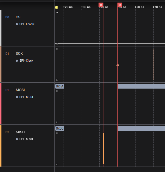
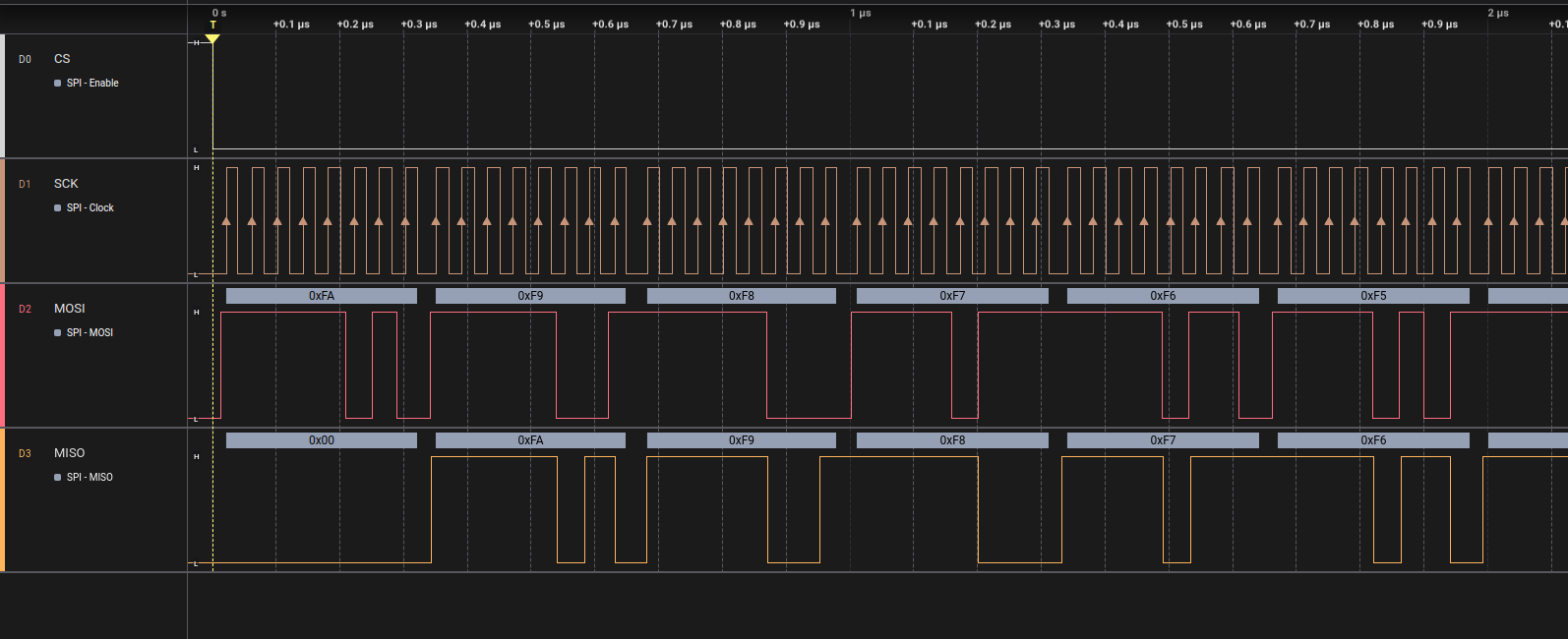
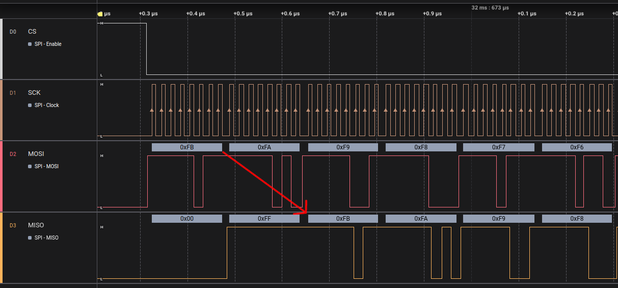
I got a fast version working. It requires that sck be connected to a clock pin though. You also can’t output data during the first byte (it’s always 0).
Data is asked for during bits 1-5 of the previous byte. This also means you can’t immediately respond to the first byte. The second byte will often be a dummy byte because of this.
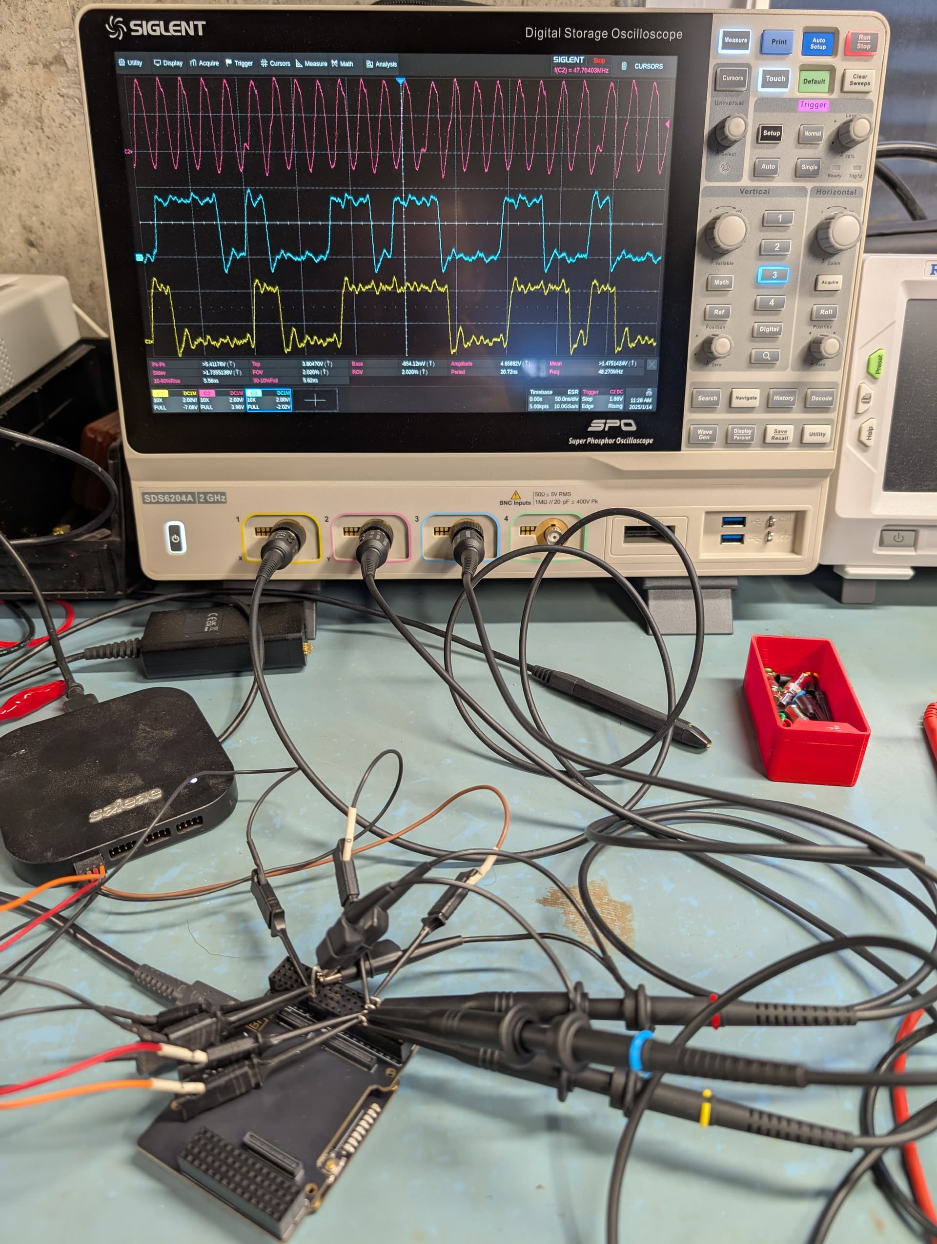
I think it should be able to get close to sck being close in frequency to the main clock. I only tested it to 25MHz as my setup was a bit spicy and signal integrity failed after that.
EDIT: I should’ve also mentioned that this requires Alchitry Labs 2.0.22 which isn’t out yet as I added arst to DFFs to support asynchronous resets. Changing the arst to a normal rst should still work as long as you always send 8 bits at a time.
Back in December I also tried this Verilog imlementation but it refused to build because the SCK pin I used was not suitable to be used as clock pin (I forget the exact wording of the diagnostic) as it was in the “wrong side” of the fabric or something like that. But I had already ordered the Teensy so I decided to try the Teensy first before I tried to understand that.
I suppose that your version will also need an appropriate choice for the SCK pin on the AU as it is used as a clock?
The old schematic is kind of a pain to check which pins are clocks but if you look at the FPGA pins you’ll see MRCC and SRCC. Those pins that are also the P variant can be used as single ended clock inputs. This is easier to see on this pinout doc.
This module clocks so few DFFs off sck it is probably safe in most cases to not use a dedicated clock pin and to route it through a BUFR.
You can do this by creating the Verilog module.
module bufr (
    input in,
    output out
);
    BUFR buffer(.I(in), .O(out)); // Xilinx built-in primitive
endmodule
Then routing sck through it.
bufr sck_buffer(.in(sck))
// use sck_buffer.out instead of sck
I updated the module some more and tested it out at 50MHz after improving my test setup.
These pins seems to correspond with the Sparkfun doc where they are labeled IO N GCLK and IO P GCLK.
Do I need something special to define one of these P pins as a clock input in the .acf file? I’d like to test that verilog implementation again, even though it explicitly states that it needs 4 times the SCK as sample clock.
Looking forward to the next release of Labs V2 too!
PS that wide Br looks very convenient to stack something else (IO or FT) on top!